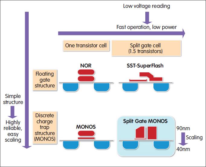
Renesas Electronics announces its successful development of the world’s first split-gate metal-oxide nitride oxide silicon (SG-MONOS) flash memory cells employing transistors with fin-shape for use in microcontrollers (MCUs) with on-chip flash memory having a circuit linewidth of 16 to 14 nanometer (nm) or finer. SG-MONOS technology is reliable for use in automotive applications and Renesas currently mass produces 40nm MCUs using this technology, and 28nm MCUs are under development. The successful development shows promising scalability of the SG-MONOS technology to 16/14nm process nodes and beyond.
Advances in automotive automation, such as advanced driver assistance systems (ADAS), and the smart society connected via the Internet of Things (IoT) have created demand for more advanced MCUs fabricated using finer process technology. To address this demand, Renesas has developed embedded flash memories based on the 16/14nm technology, which succeeds the latest 40/28nm. At the 16/14nm logic process, Fin Field Effect Transistors (FinFETs), transistors with a finned structure, are commonly employed to realize improved performance and reduced power consumption to overcome the scaling limit of conventional planar transistors.
However, employing a fin structure for embedded flash memory can become a big challenge depending on the structure of the flash memory. Two types of embedded flash memories have been proposed and implemented: the floating-gate and charge trap. Compared with floating-gate memory, the charge trap flash memory which Renesas has been utilizing in recent years has superior charge retention characteristics and a proven track record in automotive MCUs requiring a high level of reliability. Also, since the memory functional material is formed on the surface of the silicon substrate, they are comparatively easy to be extended into a three-dimensional fin structure. In contrast, floating-gate flash memory cells have a complex structure, and therefore it is difficult to integrate it into a fin structure.
Another advantage of SG-MONOS over the floating-gate structure is that the memory cell structure is maintained after replacing the dummy polysilicon gate electrode with the metal gate electrode, which is the process used to manufacture advanced logic CMOS devices with high dielectric gate insulators and metal gate electrodes.
Renesas is world’s first to successfully develop a fin-structure SG-MONOS flash memory with highly scalability, for use in high-performance and highly reliable MCUs of 16/14nm process nodes and beyond.
SG-MONOS flash memory can easily be integrated with a state-of-the-art fin-structure logic process utilizing high dielectric gate insulators and metal gate electrodes at the 16/14nm nodes and beyond, enabling massive on-chip memory capacities in the 100-megabyte (MB) range, and making possible highly reliable MCUs with over four times the processing performance of 28nm devices. Renesas will continue to confirm the operation of large-capacity flash memory based on this technology, and will move forward with development work with a view toward practical implementation around 2023.
Further information about Renesas Electronics Europe is available at http://www.renesas.com.


